Zephyr
Zephyr is an 8-bit CPU written in Verilog. The goal of this project was to explore the entire RTL-to-GDSII flow and how ASICs are made.
This helped me learn many ECE skills along the way and learn about the industry I plan to pursue a career.
The Plan
I wanted to learn about the entire process. From transistors to (relatively) high-level assembly code, and everything in between.
This meant that I had to create my own assembly language, zasm, my own compiler, interpreter, and assembler, all the Verilog code needed to describe the CPU, and utilize open-source RTL-to-GDSII flows to generate a fab-ready .gds file.
I'll go bottom-up, starting at Verilog.
Verilog
Zephyr is 8-bit, so I had to first think about what actions I wanted it to be able to perform. With two bits, I could define the CPU's four functions as NOP, LOAD, STR, and ALU. NOP is no operation, LOAD will load an 8-bit from RAM into one of Zephyr's four CPU registers (more on this later), STR will store an 8-bit value from one of Zephyr's registers into RAM, and the ALU operation will perform adding, subtracting, multiplying, and dividing operations.
Zephyr is equipped with a bank of four zregisters, R0-R3:
1module zregister (
2    input [7:0] IN,
3    input OPCODE,  // reading or writing
4    input [1:0] REG_SEL,  // which register to read/write
5
6    output reg [7:0] OUT
7);
8
9  // registers 8 bits wide, an array of 4 of them
10  reg [7:0] registers[3:0];
11
12  // reading from the register file
13  always @(*) begin
14    case (OPCODE)
15      1'b0:  // read
16      OUT = registers[REG_SEL];
17      1'b1:  // write
18      registers[REG_SEL] = IN;
19      default: OUT = 8'b0;
20    endcase
21  end
22
23endmoduleEach register can be read from or written to, depending on the OPCODE. The purpose of these registers is to give Zephyr quick access to commonly used values and as a separation from storing these values in program memory.
Zephyr also has access to a block of RAM, zram, for a whopping total of 16 words of program memory:
1module zram (
2    input [3:0] ADDRESS,
3    input [7:0] DATA_IN,
4    input OPCODE,  // reading or writing
5
6    output reg [7:0] DATA_OUT
7);
8
9  reg [7:0] registers[15:0];
10
11  always @(*) begin
12    case (OPCODE)
13      1'b0:  // read
14      DATA_OUT = registers[ADDRESS];
15      1'b1:  // write
16      registers[ADDRESS] = DATA_IN;
17      default: DATA_OUT = 8'b0;
18    endcase
19  end
20
21endmoduleLike zregister, the ADDRESS is selected, and data can be read or written from that address.
Zephyr is also equipped with an ALU to perform one of four math operations:
1module alu (
2    input [1:0] OPCODE,
3    input [7:0] DATA_A,
4    input [7:0] DATA_B,
5    output reg [7:0] DATA_OUT
6);
7
8  always @(*) begin
9    case (OPCODE)
10      2'b00:  // Addition
11      DATA_OUT = DATA_A + DATA_B;
12      2'b01:  // Subtraction
13      DATA_OUT = DATA_A - DATA_B;
14      2'b10:  // Multiplication
15      DATA_OUT = DATA_A * DATA_B;
16      2'b11:  // Division
17      DATA_OUT = DATA_A / DATA_B;
18      default: DATA_OUT = DATA_A + DATA_B;
19    endcase
20  end
21
22endmoduleIt takes a two-bit input, OPCODE, which selects what mathematical operation to perform, and 8 bits of data from two registers, storing the result of the operation on the first register, DATA_A.
The main Verilog file describes the functionality of Zephyr, which involves a state machine to synchronize every action on clock edges. Zephyr has a program counter, PC, and an instruction register, IR, to read from zram (program memory). It performs actions through three main states: FETCH, DECODE, and EXECUTE, with several others to manage ALU operations and memory writeback.
1  always @(posedge CLK or posedge RESET) begin
2    if (RESET) begin
3      // Set up all default values
4      ...
5      zstate <= FETCH;
6    end else begin
7      case (zstate)
8        FETCH: begin
9          RAM_OP   <= 1'b0;  // read
10          RAM_ADDR <= PC;
11          ZREG_OP  <= 1'b0;  // default to read
12          zstate   <= DECODE;
13        end
14
15        DECODE: begin
16          IR <= RAM_DATA_OUT;  // store fetched instruction
17          OP <= RAM_DATA_OUT[7:6];  // extract opcode
18          zstate <= EXECUTE;
19        end
20
21        EXECUTE: begin
22          case (OP)
23            2'b00: begin  // NOP
24              PC <= PC + 1;
25              zstate <= FETCH;
26            end
27
28            2'b01: begin  // LOAD
29              // Set up the memory read
30              RAM_ADDR <= IR[3:0];  // Get target addr
31              RAM_OP   <= 1'b0;  // Read operation
32              ZREG_SEL <= IR[5:4];  // Select target register
33              zstate   <= MEMREAD;  // Go to memory read state
34            end
35
36            2'b10: begin  // STR
37              RAM_ADDR <= IR[3:0];  // Set RAM addr
38              RAM_OP <= 1'b1;  // Write operation
39              ZREG_SEL <= IR[5:4];  // Select source register
40              ZREG_OP <= 1'b0;  // Read from register
41              zstate <= MEMWRITE;  // Go to memory read state
42            end
43
44            2'b11: begin  // ALU
45              ALU_OPCODE <= IR[5:4];  // Set ALU op
46              ZREG_SEL <= IR[3:2];  // Select source register A
47              ZREG_OP <= 1'b0;  // Read from register
48
49              zstate <= FETCHDATAB;  // Go to fetch data B state
50            end
51
52            default: begin
53              PC <= PC + 1;
54              zstate <= FETCH;
55            end
56          endcase
57        end
58 ...This is just a snippet of the entire state machine.
Zasm
What good is a CPU if it can't be programmed? I wrote my own flavor of assembly so that it could be highly customized to my needs. Let's walk through a simple program.
1.ORG 0
2    LOAD R0, [Y]
3    LOAD R1, [X]
4
5.ORG 14
6    DATA X, 0xDA
7 DATA Y, 0xD0The .ORG directive defines what location in program memory to start writing to. The program begins at address 0, and each new instruction will be located at the next memory location. So, LOAD R1, [X] will be stored at memory location 1.
DATA is a directive that works as a variable in zasm. Essentially, it writes the hex value to the memory location. 14 will have data 0xDA, 15 0xD0.
The instruction LOAD R0, [Y] can be interpreted as: "load into register R0 the value that the memory location Y is associated with." If we want to take a look at machine code:
1LOAD = 10
2R0   = 00
3R1   = 01
4X    = 1110
5Y    = 1111
6
7LOAD R0, [Y]  => 10001111
8LOAD R1, [X] => 10011110It is this machine code that is written to zram, which Zephyr executes instructions from. Let's look at a more complicated program:
1.ORG 0
2	LOAD R0, [X]
3	LOAD R1, [Y]
4	ADD  R0, R1
5	LOAD R0, [X]
6	MUL  R0, R1
7	LOAD R0, [X]
8	SUB  R1, R0
9	LOAD R0, [Y]
10	LOAD R1, [Y]
11	DIV  R0, R1
12
13.ORG 14
14	DATA X, 0x02
15 DATA Y, 0x05This program showcases the ALU's functionality.
RTL-to-GDSII Flow
I went with OpenROAD, an open-source tool to create .gds designs on a variety of platforms. For Zephyr, I performed the flow on the nangate45 process design kit, a 45-nanometer process, primarily because of its wide support and tooling.
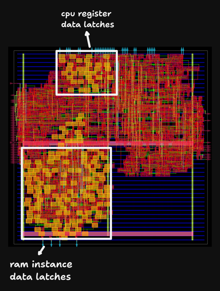
After several minutes of computation, I was greeted with this glorious design:

I've labeled the large blocks of data latches used for the four zregisters and for the zram. The rest of the components and wires relate to Zephyr's state machine and ALU functionality.
Reflection
It was an amazing experience to create this entire design, from programming language to Verilog, to transistor schematics, and I learned a ton (probably a whole class's worth of information).
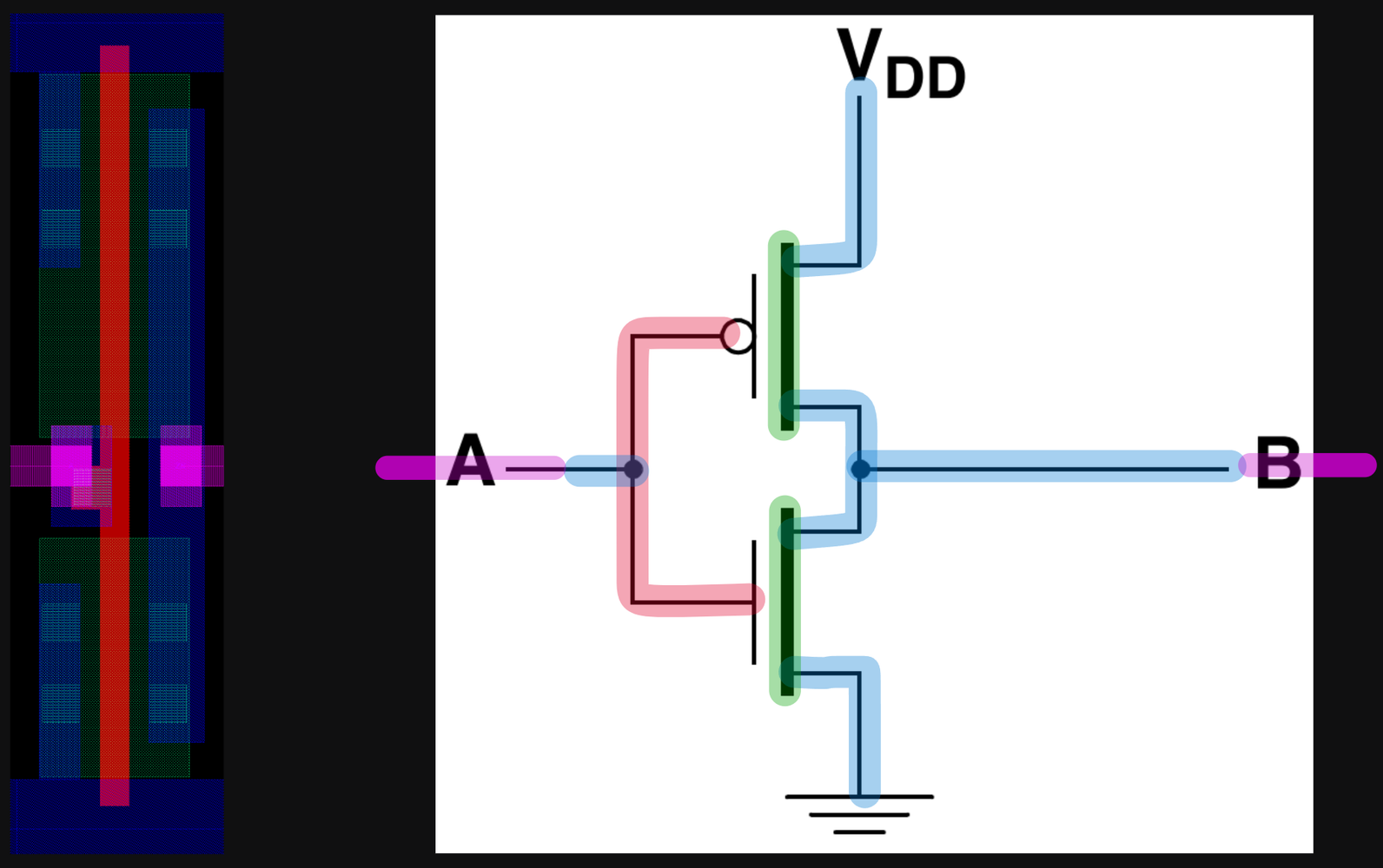
I never understood what a transistor looked like at the silicon level, but I was able to zoom right in and see the various layers of n and p-type semiconductor material, contact, metal, vias, wires, and so forth.

A diagram comparing the silicon-level design of an inverter to the commonly taught transistor schematic, with the corresponding components highlighted.
I gained a whole new insight into the microscopic world of semiconductor devices and it only further motivated me to pursue my passions and this career.